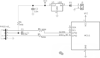
1. The connection between the
PIR and other devices should be as short as possible. On the dual panel or multi-layer board, try not to route the cable below the connection, especially if there is no large current.
2.
PIR part of the circuit as far as possible to make a separate PCB board to avoid interference. If it is done on the same board, the circuit of the
PIR part should be isolated separately and have separate grounding;
3. The VDD of the
PIR is connected to the 100NF capacitor to the ground and is as close as possible to the VDD of the
PIR.
4. The bottom of the table is coated with copper, which provides additional shielding protection and noise suppression for the inner signal, reduces the ground impedance and improves the anti-interference ability. However, if the PCB heat is large, the bottom of the
PIR tube base should not be covered with copper.
5.
PIR is recommended to have a separate LDO power supply.
PIR signal pin, power supply pins, suggested that series 100 Ω Ω - 1 k resistor.
6. The length of the
PIR pin should be as close as possible to the length of 1/2, 1/4, 1/8 of the RF source wavelength.
7. It is recommended that the
PIR be at least 3CM away from the radio source.
8. If the installation height of the
PIR on the PCB is too high, it is recommended to shield the shell.
9. The diameter of the
PIR hole on the PCB is recommended to be about 0.8mm, and the grounding pin is a heat dissipation pad.